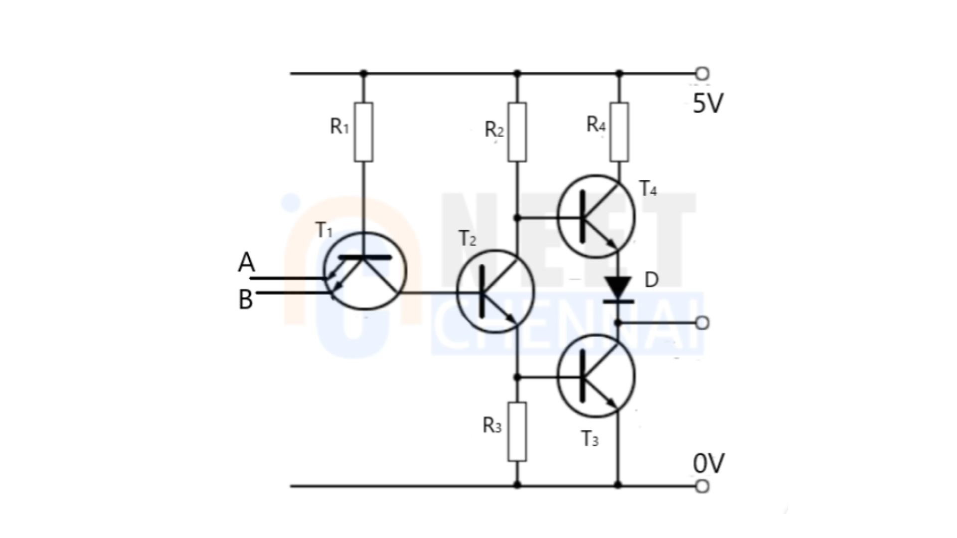
Draw the circuit diagram of TTL NAND gate and explain its working with the help of a truth table.
Hint: Recall that a NAND gate outputs 0 only when both inputs are 1. A typical TTL NAND gate logic circuit has at least four bipolar junction transistors, where the input transistor has two emitters to receive two inputs. The output is taken between the emitter and collector of different transistors.
Solution:
Explanation of Working:
The first transistor \(T_1\) has two emitters, allowing it to accept two input signals. With the base of \(T_1\) at 5V, if both inputs are also at logic 1 (around 5V), the potential difference across the base and emitters of \(T_1\) is nearly zero, so no current flows through \(T_1\), leaving it in the off state. This means the collector voltage of \(T_1\) is close to 5V, which then drives current through the emitter of transistor \(T_2\).
As current flows through \(T_2\)‘s emitter, a voltage drop develops across resistor \(R_3\), typically around 0.7V. This drop acts as the input for transistor \(T_3\), turning it on. When \(T_3\) saturates, its collector voltage drops to approximately 0.2V, which represents a logic 0 output.
For transistor \(T_4\), the emitter voltage is approximately 0.9V (0.7V from \(T_3\)‘s base-emitter voltage plus 0.2V at \(T_3\)‘s collector). Since \(T_4\)‘s base and emitter voltages are equal, \(T_4\) remains off, and the output remains low when both inputs are 1.
Truth Table for NAND Gate:
|
A |
B |
Y |
|
0 |
0 |
1 |
|
0 |
1 |
1 |
|
1 |
0 |
1 |
|
1 |
1 |
0 |
Note: In logic circuits like this, transistors typically operate in saturation mode to ensure reliable switching.


